
Project notes · 17 gen
KiCad PCB Design: How I Created My First Custom Board
For my role, project results, and current technical context, see the full project page.
Introduction
I've always been fascinated by electronics, and at some point, I realized that designing my own printed circuit board (PCB) was the next logical step. I decided to dive into PCB design with KiCad, a powerful and open-source tool perfect for both beginners and professionals. In this post, I'll walk you through the full process of designing my first custom board, sharing all the key steps, mistakes, and lessons learned along the way.
Index
Setting Up KiCad
Schematics Design
PCB Layout
Preparing for Manufacturing
Lessons Learned
Final Thoughts
1. Setting Up KiCad
Setting up KiCad was straightforward:
I downloaded the latest stable version from the official website.
During the installation, I made sure to include the official libraries (symbols, footprints, and 3D models).
I also installed a few extra plugins later, but for a first project, the default setup is more than enough.
Pro Tip: Always use the latest version for access to improved tools and bug fixes!
2. Schematics Design
Step 1: New Project I created a new project and started with the schematic editor.
Step 2: Adding Components Using the library browser, I placed all necessary components like resistors, capacitors, and a simple microcontroller.
Step 3: Wiring I connected all components using the wire tool, making sure every connection was clean and logical.
Step 4: Annotation and ERC I assigned unique reference designators to each component (annotation) and ran the Electrical Rules Check (ERC) to catch missing connections or obvious mistakes.
Bonus: I added labels to important nets like GND and VCC to keep the schematic tidy.
3. PCB Layout
Step 1: Import Netlist I switched to the PCB editor and imported the schematic.
Step 2: Component Placement I manually placed the components, thinking carefully about signal flow and minimizing trace lengths.
Step 3: Routing Routing was the fun part! I routed most traces manually, avoiding the autorouter to better understand best practices.
Good practices I followed:
Kept power traces wide enough.
Used a ground plane for better stability.
Respected minimum clearance between traces.
Minimized 90-degree trace bends.
Step 4: DRC (Design Rule Check) Before generating files, I ran the DRC to make sure everything was safe for manufacturing.
4. Preparing for Manufacturing
Step 1: Generating Gerber Files
I exported the Gerber files directly from KiCad.
Also generated the drill files needed for vias and through-hole pads.
Step 2: Verification
I used the Gerber Viewer inside KiCad to double-check everything.
Step 3: Choosing a Manufacturer
I decided to use JLCPCB because they have a simple upload process and very affordable prices for prototypes.
Bonus: I used the KiCad "Fabrication Outputs" wizard to simplify the process.
5. Lessons Learned
Designing a PCB taught me a lot! Here are some lessons I learned the hard way:
Footprint matters: Always double-check that the component footprint matches the real part dimensions.
Clearances are critical: Not leaving enough space between traces can cause shorts.
DRC saves you: Never skip the Design Rule Check before finalizing your board.
Mounting holes: Add them early! I almost forgot.
6. Final Thoughts
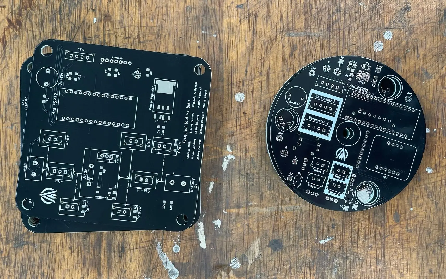
Designing my first custom PCB using KiCad was an amazing learning experience. There’s something truly satisfying about seeing your own design go from an idea on your screen to a real, physical board.
I plan to use this board in a future project, and I’m already working on new designs with more complex features.
If you're thinking about trying PCB design, just go for it! KiCad is a fantastic tool, and the experience is incredibly rewarding.